51+ sketch a stick diagram for a cmos 4-input nor gate
Web CMOS NOR Gate Circuit. It consists of parallel combination of 4 NMOS transistors that conducts when any of the input is high and pulls the output F.

Figure 4 14 From 4 Combinational Cmos Logic Circuits Cmos Logic Circuits Cmos Nor2 Two Input Nor Gate Semantic Scholar
CMOS NOR gate Stick Diagram Engineering Funda channel is all about Engineering and Technology.

. CMOS NOR gate Working 5. Vc logic 1 biases both NMOS and PMOS into conduction closing the switch and giving an electrical conduction path between A and. Web The stick diagrams uses sticks or lines to represent the devices and conductors.
Here P-channel MOSFETs Q 1 and Q 2 are connected in series and N-channel. A 3-input majority gate returns a true output if at least two of the. 34 shows 2-input CMOS NOR Gate Circuit.
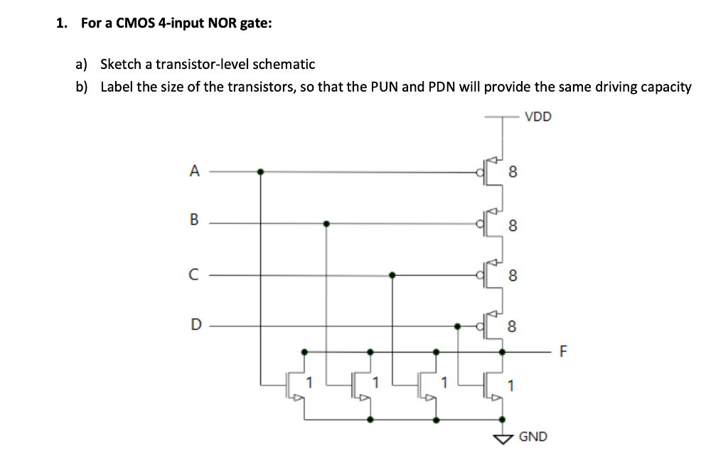
Web Design a compound CMOS logic gate for the function. Web Sheet 5 Layout and Stick Diagram 1-For a CMOS 4-input NOR gate. A sketch a transistor-level schematic b sketch a stick diagram c estimate the area from the stick.
Web CMOS Logic NOR Gates- CD4001 Quad 2-input CD4025 Triple 3-input and CD4002 Dual 4-input. Web I Draw A Stick Diagram For A 2-Input NAND Gate For Implementation Using A CMOS Process Supporting Only One Metal Layer. Web CMOS transmission gate TG.
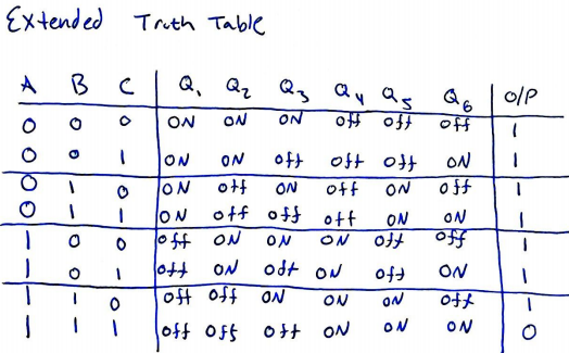
I have created a truth table next the diagram based on my understanding of basic. Web I Draw A Stick Diagram For A 2-Input NAND Gate For Implementation Using A CMOS Process Supporting Only One Metal Layer. Web The PDN of 4 input NOR gate is shown in Figure below.
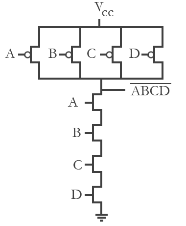
F ABCD a Sketch a transistor-level schematic b Label the size of the transistors so that the This problem has been. Web a sketch a transistor-level schematic b sketch a stick diagram c estimate the area from the stick diagram. In order to draw the layout of this circuit it is.
Figure below shows the schematic of an inverter. Web CMOS NOR gate Circuit 4. NOR gate follows Commutative but does not.
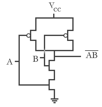
Web Someone please explain to me how the circuit below operates as NOR gate.

Pin On Electronic Schematics

Stick Diagram Of Cmos Ex Nor Gate Explore The Way Youtube

Assignment 02 Pdf Assignment 02 1 I Sketch A Stick Diagram For A Cmos 4 Input Nor Gate Ii Estimate The Area Of Your 4 Input Nor Gate From The Course Hero
Solved Vlsi Design 2 A Design A 2 Input Nor Gate And Chegg Com
E77 Lab 3 Laying Out Simple Circuits
Solved 1 For A Cmos 4 Input Nor Gate A Sketch A Chegg Com
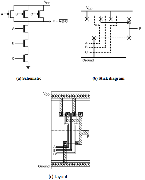
Combinational Mos Logic Circuits
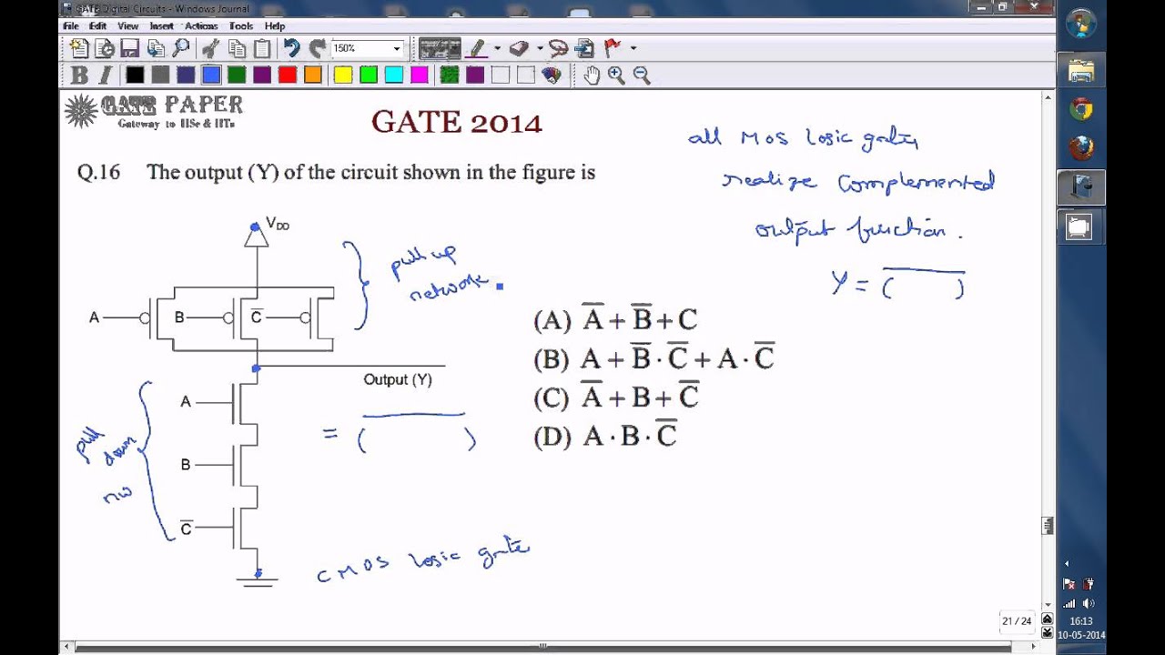
Gate 2014 Ece 3 Input Cmos Nand Gate Youtube

Sheet 5 Sheet 5 Layout And Stick Diagram 1 For A Cmos 4 Input Nor Gate A Sketch A Transistor Level Schematic B Sketch A Stick Diagram C Estimate Course Hero
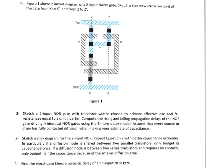
Solved Figure 1 Shows A Layout Diagram Of A 2 Input Nand Chegg Com

Cmos Vlsi Design Mips Processor Example Ppt Video Online Download
Solved Vlsi Design 2 A Design A 2 Input Nor Gate And Chegg Com
Cmos Vlsi Design Mips Processor Example Ppt Video Online Download

Sheet 5 Sheet 5 Layout And Stick Diagram 1 For A Cmos 4 Input Nor Gate A Sketch A Transistor Level Schematic B Sketch A Stick Diagram C Estimate Course Hero
Assignment 02 Pdf Assignment 02 1 I Sketch A Stick Diagram For A Cmos 4 Input Nor Gate Ii Estimate The Area Of Your 4 Input Nor Gate From The Course Hero
E77 Lab 3 Laying Out Simple Circuits
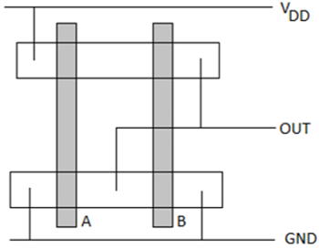
Layout Of Logic Gates Digital Cmos Design Electronics Tutorial